

The Transistor: The Tiny Switch Behind the Digital World

Look at the device you are reading this on. Inside it, billions of tiny switches are flipping on and off billions of times a second, and every one of them is a transistor. There are more transistors on Earth than any other manufactured object in history. This guide explains why the transistor replaced the vacuum tube, how a handful of physicists at Bell Labs created it, how it actually works, and how it grew from one device into the engine of the information age.
| Invented at | Bell Telephone Laboratories, New Jersey, December 1947 |
| Inventors | John Bardeen, Walter Brattain and William Shockley |
| Replaced | The vacuum tube |
| Made of | Semiconductor material: first germanium, then silicon |
| Key follow-ups | Integrated circuit (1958 to 1959), MOSFET (1959) |
| Today | Tens of billions on a single chip |
| Reading time | 10 min read |
The problem: vacuum tubes
In the early 20th century, electronics ran on vacuum tubes: glass bulbs with a glowing filament inside. Tubes could amplify a weak signal or act as a switch, which made radio, telephone networks and the first computers possible. They also had serious drawbacks. They were big, fragile, hot and power-hungry, and they burned out.
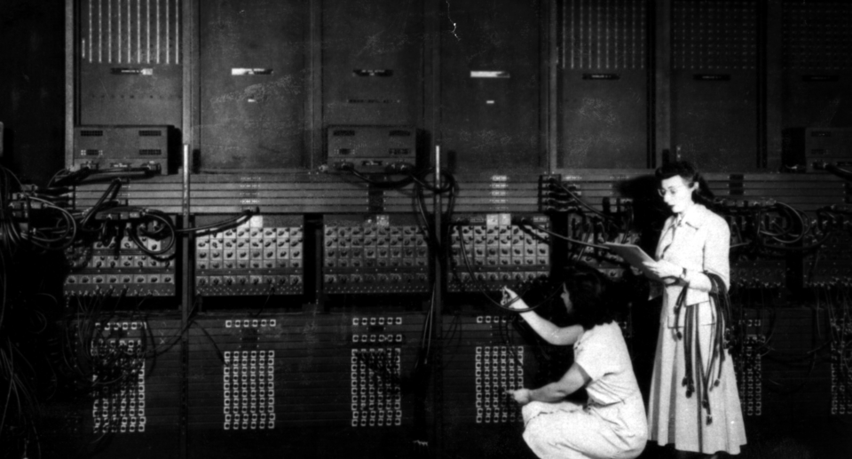
The ENIAC computer, completed in 1945 in the United States, used about 18,000 vacuum tubes, weighed some 27 tons and filled a large room. Operators spent much of their time hunting for tubes that had failed. Telephone companies faced the same problem across their networks. The call for a small, solid, reliable replacement was loud.
Bell Labs, 1947
At Bell Telephone Laboratories, the research arm of the American telephone company, William Shockley led a group studying semiconductors, materials that conduct electricity only under some conditions. Two members of the group, John Bardeen, a theoretical physicist, and Walter Brattain, an experimentalist, found that a small amount of current flowing into a carefully prepared crystal of germanium could control a much larger current. In December 1947 their device, the point-contact transistor, amplified an audio signal.
The name came from “transfer resistor”. Bell Labs announced it publicly in mid-1948. Shockley, who felt left out of the breakthrough, soon worked out a more robust design, the junction transistor. In 1956 all three men shared the Nobel Prize in Physics.
How a transistor works
A transistor has three connections. In a modern MOSFET they are called the source, the drain and the gate. Think of it as a tap: current flows from source to drain, and the voltage on the gate decides how much gets through.
Start with silicon
Pure silicon is a semiconductor: it conducts less than a metal and more than an insulator, and its behaviour can be tuned.
Dope it
Adding tiny amounts of other atoms changes how it conducts. N-type silicon has extra electrons, and p-type has missing electrons (“holes”).
Build the channel region
Two n-type regions, the source and the drain, are placed in a p-type base. Normally no current can pass between them.
Apply a gate voltage
A thin insulating layer separates the gate from the silicon. A voltage on the gate pulls electrons into a narrow channel between source and drain.
Switch on and off
With the voltage on, current flows (a 1). With it off, it does not (a 0). Tiny changes to the gate control large currents, so the same device can also amplify.
Try it: build logic from switches
A transistor acts as a switch, and switches can be wired into logic gates. The playground below shows what two input bits do under different gates. A half adder, which adds two bits, needs only an XOR gate for the sum and an AND gate for the carry.
Logic from NAND in Python
Every logic function can be built from a single gate type, NAND, which is why chip designers love it. Here are NOT, AND, OR and XOR built from NAND alone.
def nand(a, b): return 0 if (a and b) else 1
def not_(a): return nand(a, a)
def and_(a, b): return not_(nand(a, b))
def or_(a, b): return nand(not_(a), not_(b))
def xor(a, b): return and_(or_(a, b), nand(a, b))

print(" A B | AND OR XOR")
for a in (0, 1):
    for b in (0, 1):
        print(f" {a} {b} |  {and_(a,b)}   {or_(a,b)}   {xor(a,b)}")
Output:
 A B | AND OR XOR
 0 0 |  0   0   0
 0 1 |  0   1   1
 1 0 |  0   1   1
 1 1 |  1   1   0
Billions of such gates, arranged into adders, memory cells and processors, make up a computer. The binary logic of 0 and 1 also depends on the idea of zero as a number.
Shrinking the switch
1904-06: Vacuum tubes
John Ambrose Fleming and Lee de Forest develop the diode and triode tubes.
1945: ENIAC
An early electronic computer using about 18,000 vacuum tubes.
1947: Point-contact transistor
Bardeen and Brattain at Bell Labs amplify a signal with a germanium crystal.
1954: Silicon and the transistor radio
Texas Instruments makes the first commercial silicon transistor, and the first transistor radios go on sale.
1958-59: Integrated circuit
Jack Kilby at Texas Instruments and Robert Noyce at Fairchild show that several components can be made on one chip.
1959: MOSFET
Mohamed Atalla and Dawon Kahng at Bell Labs demonstrate the metal-oxide-semiconductor transistor, now the most common transistor.
1965: Moore’s observation
Gordon Moore predicts that the number of components on a chip will keep doubling at a regular pace.
1971: Intel 4004
One of the first microprocessors, with about 2,300 transistors.
2010s-20s: Billions per chip
Phones and graphics chips pack tens of billions of transistors.
The key was the integrated circuit. Instead of wiring individual transistors by hand, manufacturers could print many of them, along with the connections, on a flat piece of silicon by a photographic process. Each improvement in printing let them fit more transistors on the same chip. In 1965 Gordon Moore observed that the number of components on a chip had been doubling regularly, and the trend he described has become known as Moore’s law.
Chip makers describe each generation by a number in nanometres, such as “5 nm”. Today these names are marketing labels, not exact measurements of any one part of the transistor.
India and the chip
India has a long record in chip design, and many Indian engineers work for global semiconductor companies. On the manufacturing side, the Semiconductor Complex Limited was set up at Mohali in Punjab in 1976 and made some of the country’s earliest chips. In 2021 the government launched the India Semiconductor Mission to attract chip fabrication and assembly plants. Since then, several projects have been approved, including a chip assembly and test plant by Micron in Sanand, Gujarat, and a planned semiconductor fabrication plant by Tata Electronics in Dholera, Gujarat. Because plans and timelines change, check the official India Semiconductor Mission site for the latest status.
Mind map: the transistor at a glance
- Transistor: A tiny switch that turned electronics into computing.
- Before it: Vacuum tubes ruled.
- Fleming valve, 1904: First vacuum tube diode.
- De Forest triode, 1906: Adds amplification.
- ENIAC, 1945: About 18,000 tubes, huge and hot.
- Bell Labs, 1947: Three inventors, one idea.
- John Bardeen: Physicist.
- Walter Brattain: Experimental physicist.
- William Shockley: Group leader; junction transistor.
- Nobel Prize, 1956: Shared by all three.
- How it works: Silicon and doping.
- Semiconductor: Conducts only sometimes.
- Doping: Adding atoms to shape conduction.
- Gate controls flow: A small signal switches a larger current.
- Switch or amplifier: Two main uses.
- Shrinking it: Chips and Moore’s law.
- Integrated circuit, 1958: Kilby and Noyce.
- MOSFET, 1959: The workhorse of modern chips.
- Intel 4004, 1971: 2,300 transistors.
- Billions today: Tens of billions on one chip.
- What it powers: Almost everything.
- Computers: Logic and memory.
- Smartphones: A billion-plus switches in a pocket.
- AI hardware: Chips for machine learning.
- Solar cells: Related silicon technology.
- Before it: Vacuum tubes ruled.
Common myths
- Myth: The transistor was a single person’s invention. Three physicists shared the Nobel Prize, and many engineers improved it afterwards.
- Myth: Moore’s law is a law of physics. It is an observation about the industry’s progress.
- Myth: The first transistors were made of silicon. The first were germanium; silicon took over in the 1950s.
- Myth: Transistors only store data. They switch and amplify signals; memory is built from groups of them.
Key takeaways
- A transistor is a switch or amplifier controlled by a small voltage or current.
- It replaced vacuum tubes because it is small, cool, cheap and reliable.
- Printing many transistors on one chip (the integrated circuit) is what allowed computers to shrink.
- Logic gates built from transistors follow the same binary idea as the digit zero and one.
Frequently asked questions
How many transistors are in a smartphone?
Tens of billions in the main chip alone, plus more in memory and other chips.
Why silicon rather than germanium?
Silicon works at higher temperatures, is abundant (it is the main ingredient of sand), and forms a stable oxide layer that is ideal for MOSFETs.
Is Moore’s law over?
Progress has slowed, and shrinking is harder and costlier. Engineers now improve chips by new transistor shapes, stacking and special-purpose designs as well as by shrinking.
What is a chip made of besides transistors?
Wires and insulating layers, along with capacitors and resistors, all printed in layers on a silicon wafer.
Keep exploring
The number inside every binary code.The smartphone
Billions of transistors in your pocket.Artificial intelligence
The software that runs on those chips.
Sources
- Transistor, Encyclopaedia Britannica
- Transistor: innovation at Bell Labs, Encyclopaedia Britannica
- Integrated circuit, Encyclopaedia Britannica
- 1947: Invention of the point-contact transistor, Computer History Museum
- The Nobel Prize in Physics 1956, Nobel Prize Outreach
- India Semiconductor Mission, Government of India
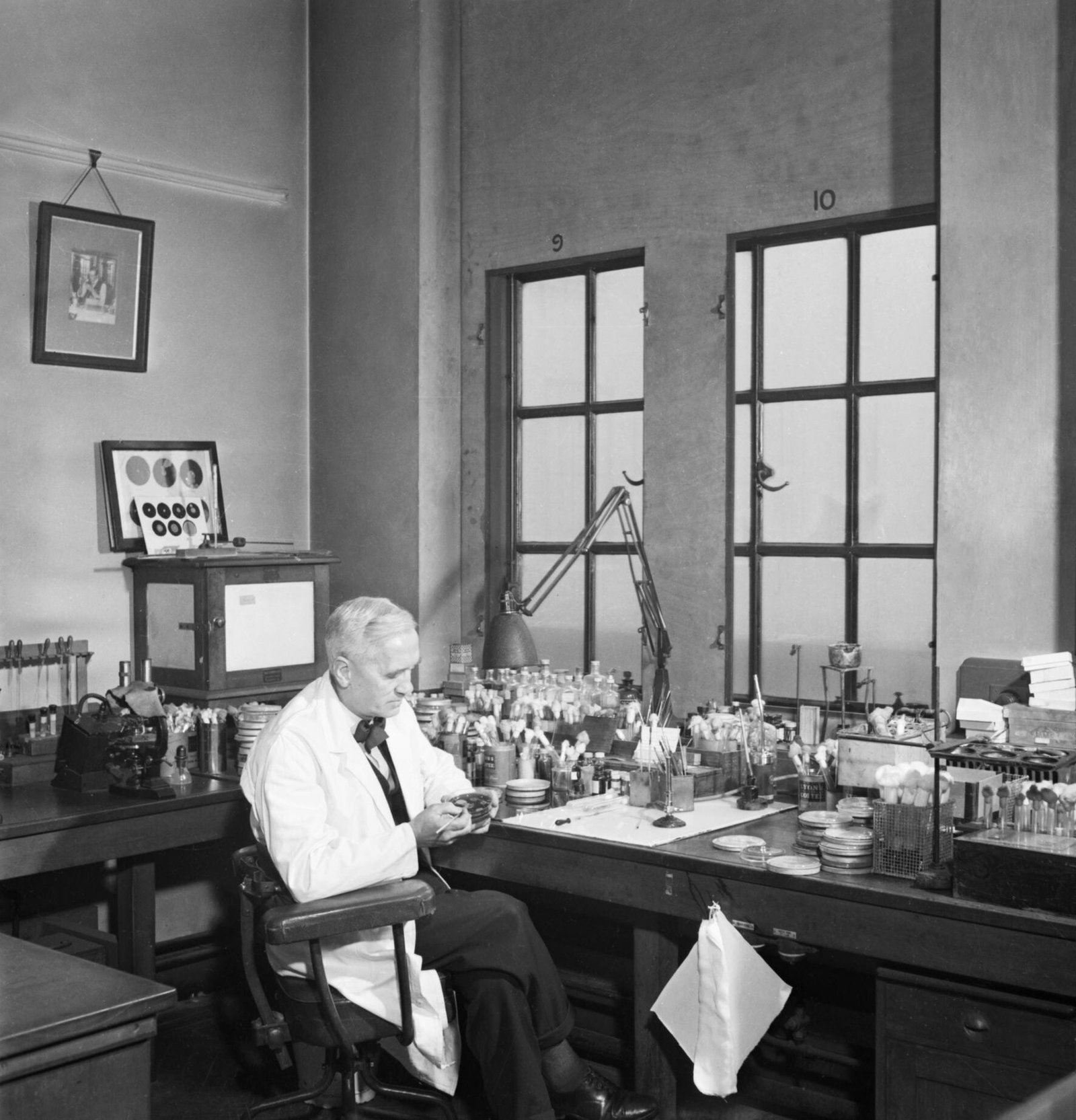
Featured image: Image: Unidentified U.S. Army photographer, via Wikimedia Commons, Public domain. Dates and counts are rounded.




4 Comments
[…] Transistor: Bell Labs, 1947: the switch behind all electronics. […]
[…] and by 2022 chatbots built on them were used by many millions of people. Chips made of billions of transistors power all of […]
[…] on zero as much as our everyday numbers do. If you want to follow that story, read our guide to the transistor, the tiny switch that stores a 0 or a […]
[…] That is only memory. Processing speed, storage and connectivity have grown by similar factors, thanks to the shrinking of the transistor. […]